I made unique business cards for myself, they are just narrow "sticks" which fit into a USB connector directly. The simplest variants can just have an ATMEGA88 chip with LED to perform 'morse code' and other types of blinkies:

However, there are more populated variants that can have their own dedicated ISP connector (1.27mm pin pitch) and with few more passives have software implemented USB HID capabilities:

One variant has soldered pin headers on the edges and is a simple, yet full dev board:

This repository is documenting the "breadboard" variant, showing the pinout of the connectors and contains a small morse code blinky project.
Note: In the images above I'm showing only one side of the PCB, the one which doesn't contain the contact details of the business card and therefore the traces for the USB connector are not visible on the photos.
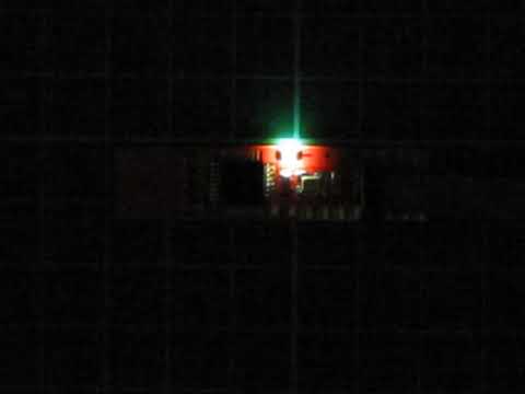
Click the thumbnail to open the video on YouTube:
There is a valid concern to plug unknown (and handmade) USB devices into your USB host. For rogue USB devices it's possible to damage the ports: USB kill USB killer Wiki
- The device doesn't contain enough HW to damage the port (no capacitors to charge up like with the USB killer)
- Full schematic is open source, see for yourself that nothing bad is done to the USB port
- Firmware is open source and the user is more than welcome to replace it with his own, the device can be reprogrammed with:
- 1.27mm ISP header
- 2.54mm J2 pin header
- with TQFP-32 pogo-pin ISP cable such as (Hobbyking's Atmel socket firmware flashing)[https://hobbyking.com/en_us/atmel-atmega-socket-firmware-flashing-tool.html] or (DIY version of the adapter)[https://www.youtube.com/watch?v=t5unHRB2sV4]
- Can use USB battery power bank (but will not be able to see and use the USB capabilities)
- The intend of the card is to presentable it would be in my best interest to not damage anything especially when on the PCB are my contact details
- If this is not enough then do not use it as a USB device, use it as a "business card" and ignore the PCB/AVR/USB capabilities

IMPORTANT NOTE: PD6 is connected directly to the LED without current limiting resistor, read below what considerations have to be made so the PIN or LED will not be damaged.
The KiCAD schematic files are stored inside KiCad/stickMk2-schematic folder
The PORTD6 is connected directly to a LED without a current limiting resistor which is a very bad design practice. But then why I did it? Because of the mk2 goals, my first mk1 revision of this stick dev board was doing everything by the spec but contained 5 components.
-
I'm always giving these away for free so I want it to be cheap Shrinking the bill of materials to 2 components not just shaved off few cents, but gave me other benefits (see below).
-
Only 2 components made the assembly faster as well. As I'm making these by hand in bulk, each step, each component adds up with 100s of boards.
This would be absolutely a no-go on real production/commercial boards, but on free boards and with few design considerations the LED can be used fairly reliably (if any problems, I offer full refunds).
The PCB has between PORTD6 and LED purposefully long and thin trace. And it's set up to drive the LED instead of sinking, these MCUs can do ~40mA when sinking, but the driving currents are weaker (~20mA). And other constraints apply too, like the combined current draw of all pins (good to read the spec). Typically the GPIOs would be set to sinking mode as that is a good practice. However, using it in the driving mode, it allows me to use the internal pull-up resistor (more in the section below).
The USB is 5V and forward voltages for LEDs are ~3.3V, the increased trace resistance and using the pin in a weaker mode is not enough. Yet there are 2 approaches how to make the LED work:
If the PORTD6 without current limiting resistor would be used as output and set to high the LED, PORT's PIN and/or MCU could be damaged.
Even when the PCB doesn't have resistors populated, there are resistors inside each IO pin (the Rpu pull-up resistors):

These resistors are not precise and according to the spec around 20k ohm to 50k ohm. Which might be on a higher side and limiting current too much (LED current is under 1mA), but it's enough to lit the LED. The input's pull-up resistor is designed to be shorted continuously so powering a LED has no effect on the port's longevity. And LED which can be driven with 20mA will be with this method driven with a current smaller than 1mA. Therefore both (port and LED) can operate within their spec and it's safe.
To turn on the LED the PORTD6 direction has to be as input with pull-up, to turn off the LED it needs to be set as input in tri-state or as output with low output. Be careful to not set the output to high by changing the DDE6 (output/input) value before changing to the correct PORTE6 (low/high and pull-up/tristate) value first.
The second risky method is PWM which is abusing the spec slightly but allows brightness control.
Use as fast PWM as possible and control the current and brightness with the duty cycle. Do not set duty cycle above 10% (in my examples I do not exceed 7% and still the LED is bright enough). It means that most of the time the LED should be powered off. Tested the board with 7% duty cycle continuously on for 100h and didn't affect brightness/draw/temperature or any noticeable aspect of operation, while the expectation of a gimmick USB dev board is expected to be used less than 100h so this looks like an OK solution, even when it's abusing the HW and the spec.
The PORTD6 is mapped as output pin OC0A for the Timer0, which can be configured to Fast PWM mode. In this mode, it's recommended to use inverted output mode as that will allow to setting OCR0A to 0xff which will result to a 0% duty cycle. While non-inverting mode and OCR0A set to 0x00 will not produce 0% duty cycle and the LED will be always slightly lit.
Warning: In this mode, it's unsafe to stop the PWM without careful timing and setting the output to a safe state before the execution is interrupted. Things like JTAG debugging would be exposing the LED to dangers where the LED could be left in a bad state for too long. The ATMEGA88 has no JTAG features and risks caused by interactive debugging can be ignored because the device has no support for debugging.
In simple terms, when using PWM extra measures have to be made to make sure it will not get stuck with the high output set for too long, but it can't be caused by a debugger.
When using either pull-up or PWM a good coding habit should be to have dedicated functions to set the LEDs states and only invoke these instead of accessing registers directly because they are simple they will get inlined (no performance penalty) and because the same functions are reused it will be less likely to make a typo and set the port register to a wrong value. See bundled source code for the blinky: main C file
KiCad schematics (pinouts of ISP, J1, J2 and full board) are stored in KiCad folder

The ISP/SPI is exposed (on J2) as well, so the device can be powered and programmed from the board J2 connector directly, or programmed from the separate ISP pin header.
| J1 | J2 |
|---|---|
| PB2 (PCINT2/nSS/OC1B) | PD6 LED (do not set output to high) |
| PB1 (PCIN1/OC1A) | VCC (5V) |
| PB0 (PCINT0/CLK0/ICP1) | GND |
| PD7 (PCINT23/AIN1) | PB5 (SCK/PCINT5) |
| PD5 (PCINT21/OC0B/T1) | PC6 (nRST/PCINT14) |
| PC4 (ADC4/SDA/PCINT12) | PB4 (MISO/PCINT4) |
| PC3 (ADC3/PCINT11) | PB3 (MOSI/PCINT3/OC2A) |
| PC2 (ADC2/PCINT10) | PC1 (ADC1/PCINT9) |

Note: This is not the typical 2.54mm pin spacing, but a 1.27mm pin-header.


| ISP1 pin | function |
|---|---|
| 1 | RST |
| 2 | GND |
| 3 | SCK |
| 4 | MOSI |
| 5 | MISO |
| 6 | VCC |
For many projects, the internal 8MHz oscillator is enough, however for the USB to work reliably, an external crystal (12Mhz for example) needs to be populated on the PCB together with two capacitors. Capacitor values depend on the crystal and, for the bundled 12MHz crystal the capacitors should be 3.3pF. For other crystals use the (capacitor load calculation)[https://www.crystek.com/documents/appnotes/PierceGateLoadCap.pdf].

To avoid unnecessary soldering on the user's side, I have prepared various variants, just ask me for a variant with the pre-populated clock/USB components.
On top of having a stable clock, 4 more passives components have to be populated on the PCB:
-
zener diodes (two 3.6V, see their orientation)

-
resistors (two 68 ohm)


I'm having various variants of the boards and these passives are already pre-populated on some of them.
The reset signal is not pulled up, in a noisy environment it's recommended to connect a pull-up resistor externally, the signal is exposed on J2 (pin 5) and ISP (pin 1) connectors.
The example project is done in CodeVision. It's a simple C project and other compilers (gcc/IAR) should be able to use the code easily: blinky source folder