This Repository contains all the information needed for physical design flow for your IPs or SOCs using qflow and other opensource tools. The Repository was created during the Beginner Physical design using open-source EDA Tools conducted by Kunal Ghosh - (VLSI System Design).
- Day-1
- IC Design Components and Terminologies
- RISC-V
- Physical Design Flow and Open source EDA tools
- Lab Exercises
- Day-2
- Floorplan
- Placement
- Cell Design Flow
- Lab Exercises
- Day-3
- ngspice Simulation
- Euler's Path and Stick Diagram
- Post-Layout extraction and Simulation
- CMOS Fabrication Process
- Lab Exercises
- Day-4
- Timing modelling using delay tables
- Clock Tree synthesis
- Timing analysis with real and ideal clocks
- Lab Exercises
- Day-5
- Routing
- DRC
- Parasitic extraction and the SPEF Format
- Lab Exercises
IC or Integrated circuit is basically an electronic circuit consisting of large number of transistors, resistors and capacitors etc inside a single semiconductor chip. They come in a variety of packages and sizes. Some of the commonly used ICs include Timer 555 ic, 741 operational amplifiers, 78xx series of voltage regulators and 74xx series of logic gates.
SOC - System on Chip is also a type of IC which has the capabilities of a computer built inside the chip. It typically consists of a CPU, memory , input and output ports, analog IPs and other units integrated within itself.SoCs can be applied to any computing task. They are typically used in mobile computing such as tablets, smartphones, smartwatches and netbooks as well as embedded systems.
Core is the section of the chip where the fundamental logic of the design is placed. Die contains the core, it is the small semiconductor material specimen on which the fundamental circuit is fabricated. IC's are fabricated on a single 9 inch or 12 inch diameter silicon wafer, which contains hundreds of mirror images of the fundamental logic. This wafer is then cut into small pieces, each piece has similar functionality of the fundamental logic called Die. Pad cells surround the rectangular metal patches where external bonds are made. input,output and power pad cells are commonly used pad cells.

Integrated circuits are put into protective packages to allow easy handling and assembly onto printed circuit boards and to protect the devices from damage. A very large number of different types of package exist. Through-hole packages, Surface mount, Chip carrier, Pin grid arrays, Flat packages and ball grid array are some of the most common packages. In this workshop we deal with a variant of Flat package called QFN-48 ( Quad Flat No leads with 48 pins)

PLLs, DAC, ADC and SRAMs come under the category of foundry IP. They have to be manually designed or need some human interference (or intelligence) essentially to define and create them. IPs(Intellectual property) are targeted on a particular technology nodes. Macros are basically digital blocks which are made up of purely digital logic.
The RISC V is an open source specification of an Instruction Set Architecture (ISA).x86 is commonly used ISA for personal computers and ARM architecture is commonly used for Mobile Phones .But these are proprietary standards Unlike most other ISA designs, the RISC-V ISA is provided under open source licenses that do not require fees to use, which provides it a huge edge over other commercially available ISAs. It is a simple, stable, small standard base ISA with extensible ISA support, that has been redefining the flexibility, scalability, extensibility, and modularity of chip designs.
Applications and softwares running in our laptops and PCs are written in a variety of languages like C, C++, Python and Java etc. These different languages cannot be directly processed and implemented by the hardware (Microprocessor Core). They need to be converted into form that is understandable by the core. This is where the ISA or the instruction set architecture (assembly language) comes into the picture. Special programs called the compiler and assembler are used to convert the instructions in different languages to the target assembly language. The compiler converts the code into assembly language, which in our case is the RISC-V ISA and the assembler takes care of converting the different instructions in textual format into binary representations which are understood by the microprocessor and executed.
with the advent of an open standard ISA like RISC-V, there are many people who have created their own microprocessor cores which are documented in the RISC-V github handle found at RISC-V Cores List.PicoRV32 is one such implementation of the RISC-V ISA created by clifford wolf. PicoRV32 is a CPU core that implements the RISC-V RV32IMC Instruction Set. It can be configured as RV32E, RV32I, RV32IC, RV32IM, or RV32IMC core, and optionally contains a built-in interrupt controller. PicoSOC is an example SOC created using PicoRV32. PicoSOC is a type of SOC flavour which is more suited towards FPGA implementation and contains a less-detailed description of memory and other Components since these are resources already available inside the FPGA.
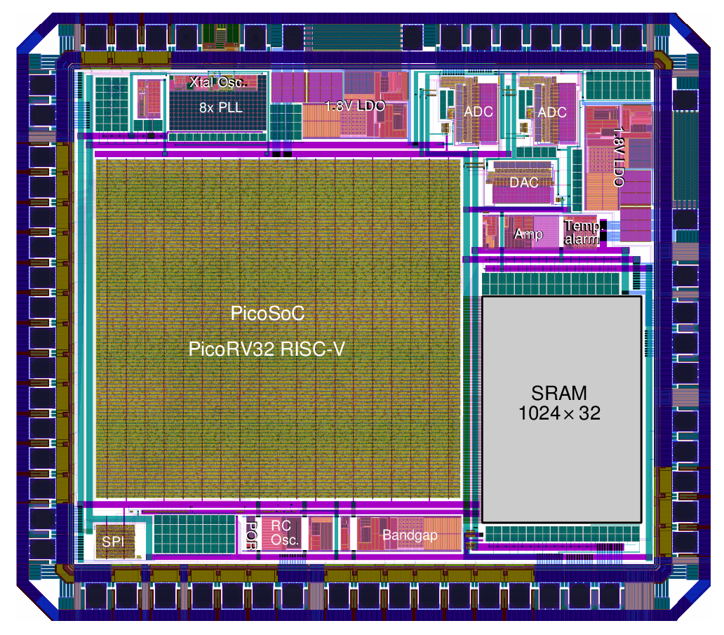
It is an ASIC implementation of the PicoSoC-PicoRV32. The core was previously proven with an FPGA implementation and Raven is the first SoC built with it.The system integrator is Tim Edwards, another champion in the open source domain. Raven includes analog IPs like PLLs (Clock Multipliers), ADCs, DACs comparators and some other blocks as well.Efabless has successfully bench-tested the Raven at 100MHz, and based on simulations the design should be able to operate at up to 150MHz.

A typical back-end flow of chip design is explained in the below section. For each step, different open-source tools were used. Qflow is a complete tool chain for synthesizing digital circuits starting from verilog source and ending in physical layout for a specific target fabrication process.The tool chain is basically a collection of steps ordered in a particular sequence that makes it easier to analyse the design as it propagates through the steps. A typical Qflow gui would look like the below picture. The steps are ordered in a sequential-order i.e, they can only be executed one after the other from top to bottom.
Logic synthesis is the process of translating and mapping RTL code written in HDL (such as Verilog or VHDL) into technology specific gate level representation. Yosys is a framework for Verilog RTL synthesis. It currently has extensive Verilog-2005 support and provides a basic set of synthesis algorithms for various application domains.
The second step in the physical design flow is floorplanning. Floorplanning is the process of identifying structures that should be placed close together, and allocating space for them in such a manner as to meet the sometimes conflicting goals of available space (cost of the chip), required performance, and the desire to have everything close to everything else.Floor planning is done using an opensource tool called graywolf as a part of Qflow.
Placement is the process of automatically assigning correct positions to predesigned cells on the chip with no overlapping such that some objective function is optimized. Placement is design state after Floorplanning and before routing. Placement also is done using graywolf as a part of Qflow.
Clock Tree Synthesis is a process which makes sure that the clock gets distributed evenly to all sequential elements in a design. The goal of CTS is to minimize the skew and latency. Clock Tree Synthesis also is done using graywolf as a part of Qflow.
Routing is the next stage after clock tree synthesis which involves making connections as per the netlist generated earlier. This includes interconnections between standard cells, macros and the Pads present in the chip boundary. Routing is done with the help of an opensource tool called Qrouter
Static Timing Analysis (STA) is one of the techniques to verify design in terms of timing.The STA will validate whether the design could operate at the rated clock frequency, without any timing violations. Some of the basic timing violations are setup violation and hold violation. STA is done using the help of Opentimer
Magic is the open source tool used for viewing and creating physical layouts for circuits after SPICE simulation. After the completion of the layout, The tool also has a facility of extracting parasitics and other delays in SPICE format which can further be simulated using spice tools
ngspice the open source spice simulator for electric and electronic circuits. It is used to create a netlist, view waveforms and calculate a rough estimate of the timing parameters. It is used both in the pre-layout and the post-layout stages for running SPICE simulations.post-layout spice simulation is done after extracting the post layout spice file using magic layout viewer.
The details of installation are well documented in the README file of https://github.com/kunalg123/vsdflow. One can install all the tools easily by following all the steps given there instead of going through the hassles of installing each tool individually.
List of tools installed using vsdflow
| Tool Name | Function |
|---|---|
| Yosys | RTL Synthesis |
| blifFanout | High fanout net (HFN) synthesis |
| graywolf | Placement |
| qrouter | Detailed routing |
| magic | VLSI Layout tool |
| netgen | LVS |
| OpenTimer and OpenSTA | Static timing analysis tool |
For installing ngspice for windows or Mac OS, it is already available as a precompiled version here. For installing ngspice in linux environments, Synaptic package manager needs to be installed first. ngspice can then be installed using the package manager.


Consider a netlist consisting of D Flip flops and logic gates. While representing the circuit as a logic diagram, different elements take different shape based on the logic functionality of the element. But in reality, all the logic gates and flipflops are rectangular or square in shape when realised as a physical layout. each of these rectangular or square blocks have a predefined area based on the target technology, in our case it is the osu018 library. The sum of all the areas of these blocks determine the dimensions (width x height) of the chip.
Utilization factor is a measure of the area occupied by the standard cells, macros and other blocks with respect to the total area of the ship. it is synonymous with packing density. Utilization factor is given by the formula (Area occupied by netlist)/(Total area of the core).100% Utilization factor indicates that there is no empty space and the netlist completely fills the core. A utilization factor of 50% means that half of the core is empty and the other half is occupied by the netlist elements
Consider a large logic block which has some blocks which are redundant. this large block can be separated into smaller blocks and this is an example of pre-placed cells. Memory, Clock-gating cell, Comparator and Mux are some of the other preplaced cells. The arrangement of these IP's in a chip is referred to as floorplanning. These IP’s/blocks have user-defined locations, and hence are placed in chip before automated placement-and-routing and are called as pre-placed cells. Automated placement and routing tools places the remaining logical cells in the design onto chip
Consider a Complex circuit powered from the source Vdd and GND. During switching operation, the circuit demands switching current i.e. peak current. Now, due to the presence of Rdd and Ldd, there will be a voltage drop across them and the voltage at Node 'A' would be Vdd' instead of Vdd. If Vdd' goes below the noise margin, due to Rdd and Ldd, the logic '1' at the output of circuit wont be detected as logic '1' at the input of the circuit following this circuit. These are referred to as noise and it is expected that the noise levels be within certain margins, otherwise the output node would go into an undefined state. There are two different noise margins commonly defined.NMl (NOISE MARGIN low) = Vil – Vol. NMh (NOISE MARGIN high) = Voh – Vih. Noise margin is the amount of noise that a CMOS circuit could withstand without compromising the operation of circuit.
To overcome the problem of Noise margins, pre-placed cells are surrounded by Decoupling capacitors. The decoupling capacitor acts as a charge storage bank and satisfies the current and voltage levels expected at the input terminals of the logic cells. Thus, the problem of voltage drop and noise levels affecting the logic levels are eliminated through the use of Decoupling Capacitors.
Consider a scenario where a driver block drives multiple signals as inputs to a load block. Say all the inputs are switching and there are a lot of nodes which are discharging from Vdd to 0 and charging from 0 to Vdd at the same time. if too many nodes charge from 0 to Vdd using the same source, then Voltage droop phenomenon occurs in which the Vdd dips to a lower value. Similarly, if too many nodes charge from Vdd to 0 using the same source, then Ground bounce phenomenon occurs in which the gnd node moves to a higher value. To avoid this issue, Vdd and gnd(Vss) metal layers form a grid like pattern over the core. Now each node would charge or discharge through different sources and the discrepancies are avoided.
Pins are basically contacts grown between the core and die borders. Clk pins have wider contacts compared to other input/output pins to decrease the resistance in it's path, since Clk is routed throughout the core.
The next step involved is binding the netlist with physical cells. A library is a collection of standard cells obtained from the foundry for a particular technology node. Each element of the netlist is mapped to a cell in the library. library consists of cells of the different functionalites like AND , XOR and D FlipFlops etc. In addition to this, it also contains different sizes of the same functional gates - representing higher drive strengths.
now the binded physical cells need to be placed inside the core. the placement is determined by the position of the input pins and the frequency of operation of the block as well. Consider a netlist operating at a very high frequency, naturally to preserve the high frequency of operation the cells must be placed very close to each other.other netlists can have regular gaps between them to avoid timing violations. if the distance between the Input/Output pins to the input or output of the netlist is more, then to preserve the signal integrity - buffers/repeaters can be added at even spacings along the path of the netlist.
As seen earlier, Libraries contain standard cells which are binded to the netlist generated. The libary contains cells with different logic functions, different sizes and different threshold voltages. Apart from this, custom cells can also be created for which the process is mentioned below.
A process design kit (PDK) is a set of files used within the semiconductor industry to model a fabrication process for the design tools used to design an integrated circuit. The PDK is created by the foundry defining a certain technology variation for their processes. It is then passed to their customers to use in the design process.
Design rules are a series of parameters provided by semiconductor manufacturers that enable the designer to verify the correctness of a mask set. Design rules are specific to a particular semiconductor manufacturing process. A design rule set specifies certain geometric and connectivity restrictions to ensure sufficient margins to account for variability in semiconductor manufacturing processes, so as to ensure that most of the parts work correctly.
A successful design rule check (DRC) ensures that the layout conforms to the rules designed/required for faultless fabrication. However, it does not guarantee if it really represents the circuit you desire to fabricate. This is where an LVS check is used. LVS checking software recognizes the drawn shapes of the layout that represent the electrical components of the circuit, as well as the connections between them. This netlist is compared by the "LVS" software against a similar schematic or circuit diagram's netlist.
A SPICE model is a text-description of a circuit component used by the SPICE Simulator to mathematically predict the behavior of that part under varying conditions. The foundry has to provide this model which characterises the performance of NMOS and PMOS devices. behavior refers to the current and voltage equations that accurately model the working of the device. Using SPICE Models is the industry standard way to simulate circuit performance prior to the prototype stage
Library and User-Defined Specifications include parameters like Cell-height, Supply-voltage, Metal-layers, Pin locations and the gate length etc.
The circuit is first designed as a spice netlist in ngspice and the different waveforms are plotted. Using the information from the waveforms, we can tweak our design paramaters such as the transistor width etc, to obtain the required timing parameters. once the spice netlist is done , the next step involved is designing the layout for the netlist.
The layout design is done through Magic layout tool , and it is designed in such a way that the DRC rules are satisfied. Before layout is designed, an intermediate step called stick diagram could help to visualise the rough layout. stick diagrams are a means of capturing topography and layer information using simple diagrams. Stick diagrams convey layer information through colour codes (or monochrome encoding). Acts as an interface between symbolic circuit and the actual layout. stick diagrams can be drawn in any order (the order of the inputs), but designing using Euler's path results in less congestion and a neat layout. An Euler path, in a graph or multigraph, is a walk through the graph which uses every edge exactly once. The order of the inputs obtained from the Euler's Path is then used to design the layout.
Cell characterization is a process of analyzing a circuit using static and dynamic methods to generate models suitable for chip implementation flows. Cell characterization typically takes cell design extracted as spice circuit and spice technology models. Characterization software like guna from Paripath, analyzes this information to
- acquire or recognize cell’s function,
- generates stimulus appropriate to determine characteristic (like delay, transition time etc),
- simulates it using circuit simulator,
- gather simulations output to measure characteristic and
- finally writes this data into a standard like libertyTM, veriog or IBIS. To conclude Cell characterization, Softwares like GUNA take the spice model as inputs and create timing, noise and power .libs and functions .
Slew low (Time for 20% of Vdd), Slew high (Time for 80% of Vdd) , Input and Output are also time characterized for both rising and falling transitions. This can be manually done by viewing the waveforms in ngspice and obtaining the difference between the coordinates in the input and output waveforms.
| Timing Threshold Definitions | Percentage of Vdd |
|---|---|
| slew_low_rise_thr | 20% |
| slew_high_rise_thr | 80% |
| slew_low_fall_thr | 20% |
| slew_high_fall_thr | 80% |
| in_rise_thr | 50% |
| in_fall_thr | 50% |
| out_rise_thr | 50% |
| out_fall_thr | 50% |
Propagation Delay is a measure of time taken by the signal to pass through a gate. It is calculated with the help of parameters like in_rise_thr ,in_fall_thr, out_rise_thr and out_fall_thr. The propagation delay is basically the time difference between the input crossing 50% and the output crossing the 50% point. The propagation delay is expected to be positive and if it comes out to be negative - it means that the transistors are not properly sized or the threshold voltage setting is faulty. This is an important factor in circuit design that must be kept in consideration before designing a logic circuit in spice
Transistion time is the time needed for a signal to pass from 10% to 90% or from 20% to 80% of its final state. The delay of a cell can be deduced from the standard cell library, it is a function of input transition time and output capacitance load.The input and output slew can be found using ngspice waveforms by locating the 20% and 80% points and subtracting them


Inverter model was created as a spice deck and simulations were run on the model.ngspice was used to obtain the transfer characteristics(Input voltage vs Output Voltage) and transient analysis (Input and Output Voltage vs Time). Different delay parameters were calculated using the plots obtained from ngspice.
As discussed earlier, Euler's Path provides an improved stick diagram and subsequently the layout. Euler's path provides the order in which the inputs are to be arranged in the final layout. A non-euler based design and euler path based design for a same logic function was performed and it proved that using Euler's path provides lesser congestion between the metal layers and more optimised layout.
The layout can be drawn manually through Magic layout tool or can be automated with the help of scripts written in tcl.Once the layout is complete, the input nets are labelled by clicking on the gates followed by post layout extraction. Post layout extraction of SPICE model gives more insights regarding the parasitics that occur after creating the layout. the spice deck is run and the plots are looked again to verify that there is some difference between the pre-layout and the post layout simulations.
16-Mask CMOS Process summary:
- Selecting a substrate.
- Creating active region for transistors
- N-Well and P-Well formation
- Formation of ‘gate'
- Lightly doped drain(LDD) formation
- Source and drain formation
- Steps to form contacts and interconnects(local)
- Higher level metal formation


The switching threshold with pmos width of 0.5u is about 1.07 V as visible from the waveform below


The switching threshold with pmos width of 0.75u is about 1.17 V as visible from the waveform below


delay tables are tables which represent the delay of a gate as a function of input slew and output capacitance. As discussed before many standards cells of different sizes would be present in the library. to calculate the propagation delay across these cells, the delay table is used. if a value for a particular output load and an input slew is not present in the table, it is usually extrapolated from the nearby values present in the table. A typical delay table looks like the one given below Delay Table for CBUF'1'
| Input Slew\Output Load | 10fF | 30fF | 50fF | 70fF | 90fF | 110fF |
|---|---|---|---|---|---|---|
| 20ps | x1 | x2 | x3 | x4 | x5 | x6 |
| 40ps | x7 | x8 | x9 | x10 | x11 | x12 |
| 60ps | x13 | x14 | x15 | x16 | x17 | x18 |
| 80ps | x19 | x20 | x21 | x22 | x23 | x24 |
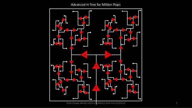
Clock Tree synthesis is the next step after placement. Clock signals cannot be routed in the same way other data signals are routed because all the sequential elements in a particular stage expect the clock edges at the same time, in other words the clock skew should be zero.To achieve this clocks are routed in a h-tree fashion, instead of directly connecting the clk pins to the clk input of the sequential elements. Also at every level of the clock path , the load driven must be same inorder to ensure synchronous working of all the cells. this is maintained by using same type of buffer cells throughout a particular stage.
Static timing analysis determines whether there is any setup or hold violations in the circuit. With ideal clocks, the analysis becomes easy, since the clk arrival time is definite and not subject to change. but in real scenarios, clk signals have noise and some uncertainity associated with it due to a variety of factors. Clock shielding can be done to prevent the noise impact on the clk signals.


One of the most popular routing algorithm called Lee's algorithm or maze routing was explained during the workshop. The process starts from the driver and all the surrounding grids to the driver cell are numbered 1. then all the adjacent cells to cells numbered 1 are numbered as 2 and this process is repeated until the target grid is reached. now, there may be multiple paths between the source to the destination, but the one with the least number of bends is preferred .
Some rules regarding the metal layers need to be followed carefully to avoid DRC failure. Consider a pair of wires in the same metal layer,they are expected to maintain a minimum width, pitch and spacing between them. Two wires from different source to different destination should not intersect in the same metal layer. they have to be separated into different metal layers to avoid shorting. while doing so, rules like the specified Via Width and Via Spacing must be maintained.
Parasitic Extraction is calculation of the parasitic effects in both the designed devices and the required wiring interconnects of an electronic circuit: parasitic capacitances, parasitic resistances and parasitic inductances, commonly called parasitic devices, parasitic components, or simply parasitics. The major purpose of parasitic extraction is to create an accurate analog model of the circuit, so that detailed simulations can emulate actual digital and analog circuit responses. Digital circuit responses are often used to populate databases for signal delay and loading calculation such as: timing analysis; power analysis; circuit simulation; and signal integrity analysis. Analog circuits are often run in detailed test benches to indicate if the extra extracted parasitics will still allow the designed circuit to function.
SPEF Format Standard Parasitic Exchange Format (SPEF) is an IEEE standard for representing parasitic data of wires in a chip in ASCII format. Non-ideal wires have parasitic resistance and capacitance that are captured by SPEF. These wires also have inductance that is not included in SPEF.


- Kunal Ghosh, Co-founder (VSD Corp. Pvt. Ltd)
- Nickson P Jose, Teaching Assistant (VSD Corp. Pvt. Ltd)