This project introduces an architecture that optimizes Stencil Kernel Calculations and is offloaded to FPGAs with the use of Vitis (Vivado) High Level Synthesis tool (HLS).
Project is created with:
- C/C++
- Vitis HLS 2021.2
- Run Vitis (or Vivado) HLS adding the source & header files from the corresponding folder.
- The different no. of CKs is denoted as K.
- The no. of Time-Steps is denoted as D.
- Each folder contains a version of the architecture with different factors K and D.
- The jacobi9d.cpp file should be used as the top function for the implementation of a single time-step.
- The SpatioTemporal.cpp file should be used as the top function for the implementation of multiple time-steps.
- Utilize the provided Test-Bench from the corresponding folder.
- In the header file the defined size of the grid can be modified.
- The number of Time-Steps can be modified in the Temporal.cpp file, by adding succesive calls to the jacobi9d funncion and declaring the intermediate variables.
- The number of CKs available requires modifications to the code of jacobi9d.cpp by adding/removing blocks that describe the Reuse Chains.
This architecture is based on the work done in [1] which in turn is an expansion on [2]. The challenge that this design addresses is the optimality of the design when more than one Computation Kernels (CKs) are used in a single stage, where a CK is a compute module that implements the kernel function. That means that more than one inputs are processed at each clock and more than one outputs are produced by the design. Essentially, [1] introduces an optimal design that exploits spatial parallelism, i.e., the concurrent calculation of results within the same clock cycle.
This architecture proposed in [1] retains the properties that the architecture in [2] achieves and extends them to a design with multiple CKs. Firstly, the design is fully pipelined, meaning that the CKs are able to consume one new input every clock. Additionally, it fully reuses the input data so that they only need to be fetched once from external memory, as well as creating a memory system with the minimum reuse buffer size. It is important to note that the input elements are lexicographically ordered and streamed into the design. The architecture developed computes a 9-Point Jacobi kernel, therefore the structure presented below is dedicated to the stencil pattern of a 9-Point stencil (square).

The figure above provides an overview of the accelerator. Given that 𝑛 is the arbitrary number of CKs, the design inputs 𝑛 new data from external memory, these inputs are concurrent, i.e., they happen simultaneously through 𝑛 different input ports at the same clock cycle. At the next cycle 𝑛 new inputs are introduced and so forth, ensuring the streaming of data in every port. These data are introduced to the memory system that feeds the CKs with the appropriate data. Then 𝑛 results are calculated in the respective kernels and are forwarded to the Output Handler. In turn, the Output Handler, determines whether data should be outputted, if that is the case, it decides to output either from the CKs, or directly from the memory system, in case of halo data. The operation of the Output Handler ensures streaming output of data, in lexicographic order.

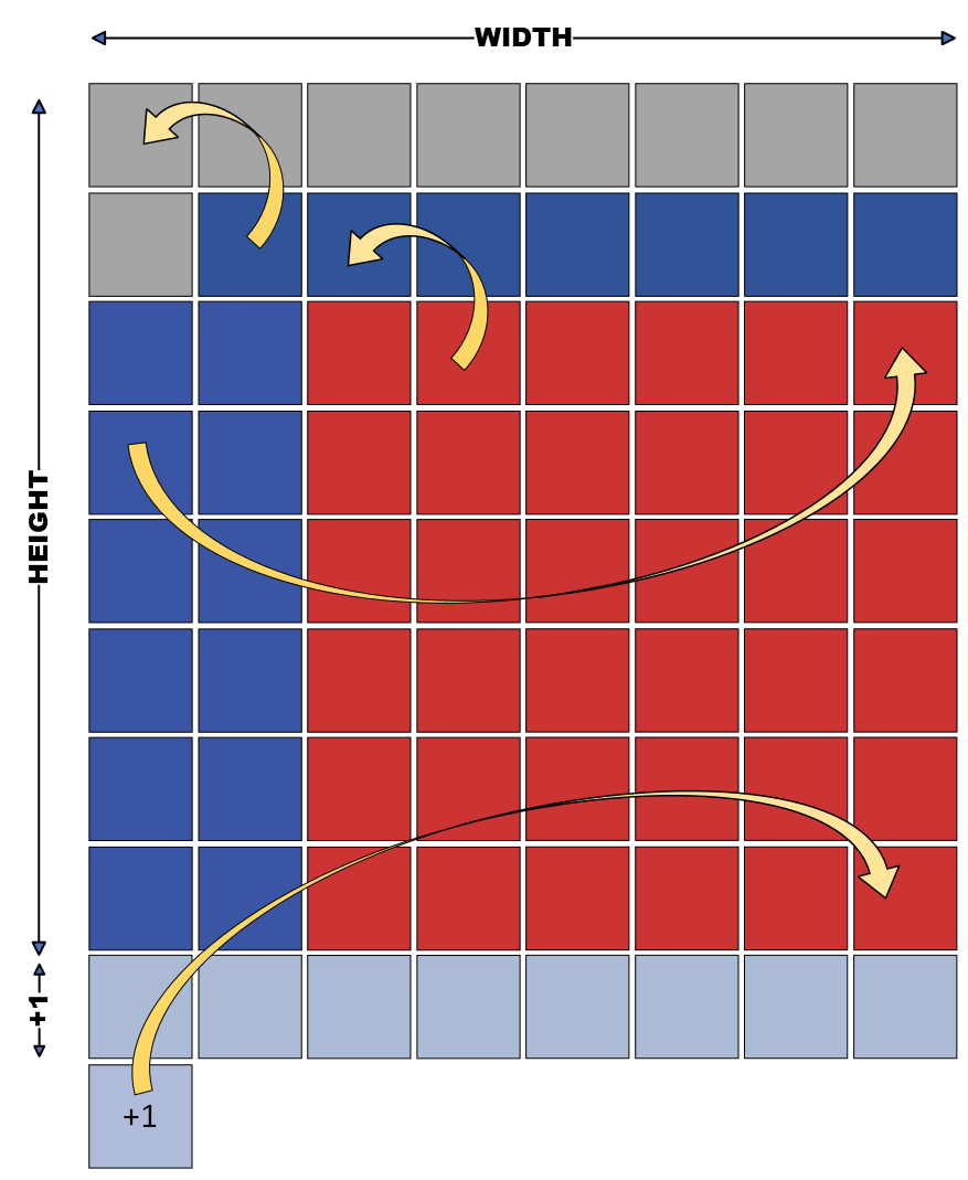
An example of 𝛫 = 4 CKs available, hence 4 concurrent computations, will be considered. The figure presents a 2-dimensional grid 𝐴, of dimension size 𝐻𝐸𝐼𝐺𝐻𝑇 and 𝑊𝐼𝐷𝑇𝐻 with their corresponding iteration variables being 𝑖 and 𝑗. Note that the iteration starts at " − 1" for both dimensions, this is a design choice that has to do with the layout of the created memory system. Moreover, the iteration step is equal to 𝑛, so as to have 𝑛 elements processed in each clock cycle. The width of the array is denoted as 𝑊 and the numbering written on the cubes marks iteration distances among them using as starting point the element in [0,0]. To ensure the correct operation of the design, it is essential that 𝑛 should perfectly divide the total width of the innermost loop of the stencil kernel, i.e., 𝑊𝐼𝐷𝑇𝐻.
The elements required for the computation of 𝑛 results are represented as the cubes highlighted in red. The ones that are stored on-chip without contributing to the calculation of the current clock cycle are highlighted in green. The sum of the highlighted cubes represents all the elements that need to be stored in internal memory. The opportunity to reuse these data manifest itself as most of them take part in more than one computation. The memory system carries out this task. Elements are divided into 𝑛 sets, according to their iterator’s remainder modulo 𝑛, as described in the following equation.
𝑗 % 𝑛 = 𝑥
In the example of n=4 where the data needed for calculation are named and highlighted in red, the resulting data sets of Equation the equation above are presented below.
𝑗 % 4 = 3 ⟶ {−𝑊 − 1, −𝑊 + 3, −1, 3, 𝑊 − 1, 𝑊 + 3}
𝑗 % 4 = 2 ⟶ {−𝑊 + 2, 2, 𝑊 + 2}
𝑗 % 4 = 1 ⟶ {−𝑊 + 1, 1, 𝑊 + 1}
𝑗 % 4 = 0 ⟶ {−𝑊, −𝑊 + 4, 0, 4, 𝑊, 𝑊 + 4}

These 𝑛 sets are called Reuse Chains and considering that for each clock cycle the design inputs 𝑛
elements and generates 𝑛 consecutive output elements, it becomes apparent that each new element is
introduced to a corresponding chain. The Figure above accurately maps the how the data elements of the example
in the previous Figure are fed in

The collection of these Reuse Chains makes up the memory system. The memory system is referred to as the Reuse Buffer and, for an arbitrary number 𝑛 of CKs available, is presented in the above Figure. The Reuse Chains are further fragmented into memory elements, either registers or FIFOs. The data elements in the Reuse Chains that need to be available for computational purposes in an arbitrary clock cycle, are stored in registers, that are denoted as 𝑅_0, 𝑅_1, etc. The need for parallel access to these elements in order to propagate their values to the CKs, justifies the use of independent memory units. The rest of the data are destined for computations in following clock cycles, and thus are stored in FIFOs. With every clock cycle the data are shifted through each reuse chain. One new input is introduced, each memory unit feeds the following and receives new input from the previous one, therefore the values inside the FIFOs are shifted and new elements that are ready to be forwarded to the CKs, are available in the registers.
Since the numbered elements in each set have the same remainder modulo 𝑛, the minimum iteration distance between them will be 𝑛. If the interval length equals to 𝑛, then the elements are stored in consecutive registers (e.g., elements −𝑊 − 1 and −𝑊 + 3 are separated by distance 𝑛 = 4, thus are stored in consecutive registers in the red reuse chain, as shown in the previous Figure). If the interval length exceeds 𝑛 then the intermediate elements are stored in the FIFOs.
An important distinction among the Reuse Chains is present in the architecture and depicted in the Reuse Buffer figure
and classifies them in two categories. The first
A better understanding of the individual memory elements that each category utilizes is available on the tables bellow. The first table provides an overview of data stored in the first Reuse Chain, when considering the example of Figure 17 where 𝑛 = 4. The last Reuse Chain is structured in the same manner. On FPGAs, large FIFO, whose capacity exceeds 1024 bits is implemented with BRAM and small FIFO is implemented with SRL.

The size of the FIFOs can be derived as follows. Between element −𝑊 + 7, which will be the first
element stored in the FIFO_0, and −1, the iteration distance is $ −1 − (−𝑊 + 7) = 𝑊 − 8$ or
$$ FIFO{edge_{size}}={WIDTH-2*n\over n } = {{WIDTH \over n} -2 } $$
This result is apparent in the Grid Map Figure where the FIFO stores every 𝑛^𝑡ℎ data element in the first row, except from the first two. The total size of the Reuse Chain is the aggregate of the sizes of all the individual memory elements in that buffer. In the case of the first and last chain, that is:
$$ Chain{edge_{size}}={{2WIDTH\over n} -4 +6}={{2WIDTH\over n} +2} $$
Which in turn is also evident in the Grid Map Figure, as the edge Reuse Chains store every 𝑛^𝑡ℎ data of the first and second rows, as well as 2 elements from the third. The second table presents the synopsis of the first intermediate buffer and the individual memory elements in which it is broken down. The table examines the Reuse Chain highlighted in color blue, in the Grid Map Figure, although all intermediate chains follow the same layout.

The FIFOs of these Reuse Chains store every n^th data element of a row except from one element. The first element in the first FIFO,
as presented in the Grid Map Figure, will be the one named
$$ FIFO{intermediate_{size}}={1-(-W+5)\over n}={(W-4)\over n}={(W-n)\over n}={{WIDTH\over n}-1} $$
Where W denotes the WIDTH of each row. As follows, the sum of individual memory element sizes makes up the total size of the intermediate Reuse Chain.
$$ Chain{intermediate_{size}}={{2WIDTH\over n}-2+3}={{2WIDTH\over n}+1} $$
Where the assumption that n>1 has been made, ergo, there are 2 edge Reuse Chains and n-2 intermediate ones.
Considering the example of the Grid Map Figure where n=4 and utilizing the equation above we conclude that the whole buffer has a total size of
The Output Handler of the design mimics the function of the one of STSA. It receives data from the Computation Kernel and utilizes control logic to decide whether to forward data to the output ports, as well as deciding the nature of these data, that is, halo or computed data. It should be emphasized that a delay is introduced in the output of the calculated data. Given the fact that n results should be outputted simultaneously, along with the need to input the element at the position [i+1,j+1] in order to calculate the result at position [i,j], creates a subsequent delay of (WIDTH+1)/n. The divisor n is a result of the iteration step that has the same size. In the example presented in Figure 16, the first n=4 outputs of the CKs are available once the element named W+4 is read. Subsequently, elements named 1 through 4 are outputted. The control logic of the Output Handler ensures the continuous flow of data in the output ports by introducing the same delay, of WIDTH+1 clock cycles, to the output of halo data. The aforementioned data are already situated inside the reuse chains in registers R_1 and R_2 for intermediate and edge chains respectively. In order to better understand the output delay.
It should be noted, that alike the TCAD architecture, the SODA has an intrinsic latency.
This is the time measured in clock cycles, necessary to forward data to the CK’s from the Reuse Buffer, compute the results and output the calculated data.
This intrinsic latency is measured from the cycle that the data required for a computation is read,
until the computed value is outputted, and will be denoted as SPTA_Latency.
Therefore, for the total latency of the design, all the grid elements should be traversed, ergo
where the term

The architecture described up to now computes the Jacobi 9-Point stencil kernel for a single timestep. To extend this work and implement iterations in the time domain, a simple approach would be to replicate the hardware of the design, thus creating multiple stages, and cascading them together. The outputs of the first stage will be the inputs of the second and so forth. The Figure above provides an overview of a complete Cascaded SPTA architecture where two stages are cascaded. The overhead in hardware is the individual channels that are created between the stages, depicted as blue boxes, in addition to the replicated hardware of each stage. These channels are implemented as simple FIFOs and contain control signals that inform the next stage about the availability of data, generated by the previous stage. Therefore, the model is completely data driven.

It ought to be noted that the succeeding stages do not wait for the completion of the previous ones to initiate their operation. Contrary they start once their input data is available, ergo the stages work in a parallel fashion. Figure 20 is an abstract representation of that type of parallelism, the first outputs of the stage will be forwarded to the intermediate channels and then fed to the next stage. The streaming property of a single stage, i.e., the ingrained ability to produce and consume 𝑛 data every consecutive clock cycle, ensures that following stages can have new inputs available for every clock. Consequently, the design of Cascaded SPTAs behaves in a streaming manner.
The total latency of a CSPTA design with 𝑘 stages cascaded, is the aggregate latency of the last design
along with the latency that the 𝑘 − 1 previous ones need to output the first set of data elements. The following equation
describes the total latency of one stage. The stencil kernel iterates over a 2-dimensional grid of size
[1] Y. Chi, J. Cong, P. Wei and P. Zhou, "SODA: Stencil with Optimized Dataflow Architecture," 2018 IEEE/ACM International Conference on Computer-Aided Design (ICCAD), 2018, pp. 1-8, doi: 10.1145/3240765.3240850.
[2] Cong, Jason & Li, Peng & Xiao, Bingjun & Zhang, Peng. (2014). An optimal microarchitecture for stencil computation acceleration based on non-uniform partitioning of data reuse buffers. 1-6. 10.1109/DAC.2014.6881404.